MASTIR VE DOKTORA ADAYLARI
LOOKING FOR MOTIVATED MSc. and PhD. Candidates
Contact persons: Prof. Dr. Nihan Kosku Perkgöz (NKP), Prof. Dr. Feridun Ay (FAY)
Department: Electrical and Electronics Engineering Department
e-mail: nkperkgoz@eskisehir.edu.tr & feridunay@eskisehir.edu.tr

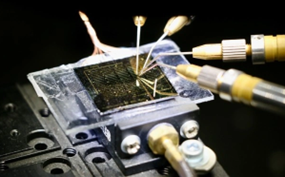
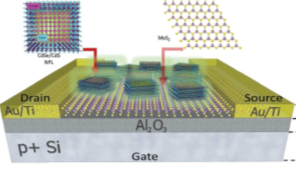
Our Research Group: The fully equipped MIDAS (Micro/nano Devices and Systems) laboratory (360 m2) houses a standard clean room environment and an infrastructure established aiming for the design, fabrication and analysis of various materials and devices including photodetectors, transistors, waveguides, supercapacitors, and sensors. MIDAS Group operates in the field of nanoelectronics and photonics: device fabrication, optoelectronic characterization and test laboratory, and nano-materials (such as graphene, transition metal chalcogenides, MXene) growth laboratory (by chemical vapor deposition- CVD). Among the equipments, atomic layer deposition (ALD/PEALD), plasma assisted chemical vapor deposition (PECVD), reactive ion etching (ICP-RIE), thermal coating, reactive ion etching (ICP-RIE), mask aligner, confocal Raman spectroscopy, atomic force microscopy, mechanical profilometer, Fourier transform infrared spectroscopy, optical microscopes, optoelectronic probe station, SR830-Lock in amplifier, prism adapter- Metricon 2010/ M, unique fiber and waveguide measurement setup and adjustable laser source (300 -1400 nm) – NKT.
MIDAS has participated in various national projects aiming for 2DM integrated aircraft components and single photon generators based on 2DM for quantum computing technologies.
 Expected contribution: We have ongoing projects and collaborations in the field of optoelectronics and nanotechnology where we need large-area and controlled production of various 2D materials (such as graphene, MXene, transition metal chalcogenides) using chemical vapor deposition (CVD) and design-implementation of different optoelectronic devices.
Hence, we expect the candidate to undertake a growth, transfer, and device fabrication tasks.
Depending on the background of the candidate, the tasks can be reconfigured to focus mostly on one of the aspects such as material growth, its characterization, device fabrication and their implementation. Hence, candidates with the background in electronics engineering, physics, material science and nanotechnology are welcome.
Please contact us by email.


